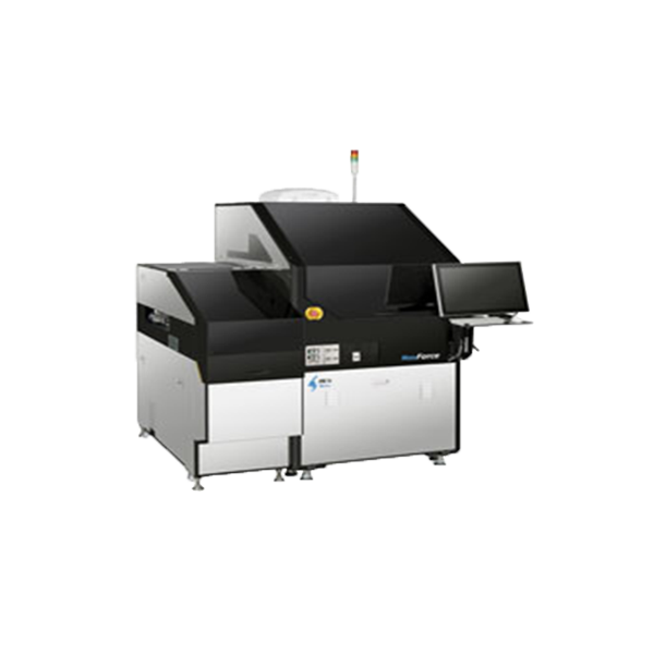
Package Bonder FPB-1s NeoForce

Manufacturer:  Shinkawa

Model No.:  FPB-1s NeoForce

Specifications

• Bond Process Handling Capability: TCB (NCP/NCF/TC-CUF), C2 and C4, FO-WLP
• Bonding Accuracy: ±2.5μm(3σ)based on Shinkawa standard bonding conditions
• Machine UPH: UPH6,000 (C4 mode/process time not included) based on Shinkawa standard bonding conditions
• Bonding Force: 0.3 – 350N
※The bonding process can select either low force control or high force control; no switchover during a single bond profile.
・Low force control mode:0.3 – 20N
・High force control mode:10 – 350N
• Bonding Tool Setting Temperature: RT – 400℃ (1℃/Step, Pulse heat)
• Bonding Stage Setting Temperature: RT – 110℃ (1℃/Step)
• Chip Size: □1 – 22mm t=0.02 – 0.7mm
• Chip Wafer Size: φ200mm, φ300mm
• Substrate Size: L : 120 – 300 mm, W : 40 – 200 mm (Max 450mm option), t : 0.2 – 2.5 mm
• Bonding Direction: Face down/Face up (Option/Other conditions available on request)

Package Bonder FPB-1s NeoForce

Manufacturer:   Shinkawa

Model No.:   FPB-1s NeoForce

Specifications

• Bond Process Handling Capability: TCB (NCP/NCF/TC-CUF), C2 and C4, FO-WLP
• Bonding Accuracy: ±2.5μm(3σ)based on Shinkawa standard bonding conditions
• Machine UPH: UPH6,000 (C4 mode/process time not included) based on Shinkawa standard bonding conditions
• Bonding Force: 0.3 – 350N
※The bonding process can select either low force control or high force control; no switchover during a single bond profile.
・Low force control mode:0.3 – 20N
・High force control mode:10 – 350N
• Bonding Tool Setting Temperature: RT – 400℃ (1℃/Step, Pulse heat)
• Bonding Stage Setting Temperature: RT – 110℃ (1℃/Step)
• Chip Size: □1 – 22mm t=0.02 – 0.7mm
• Chip Wafer Size: φ200mm, φ300mm
• Substrate Size: L : 120 – 300 mm, W : 40 – 200 mm (Max 450mm option), t : 0.2 – 2.5 mm
• Bonding Direction: Face down/Face up (Option/Other conditions available on request)
TOP