

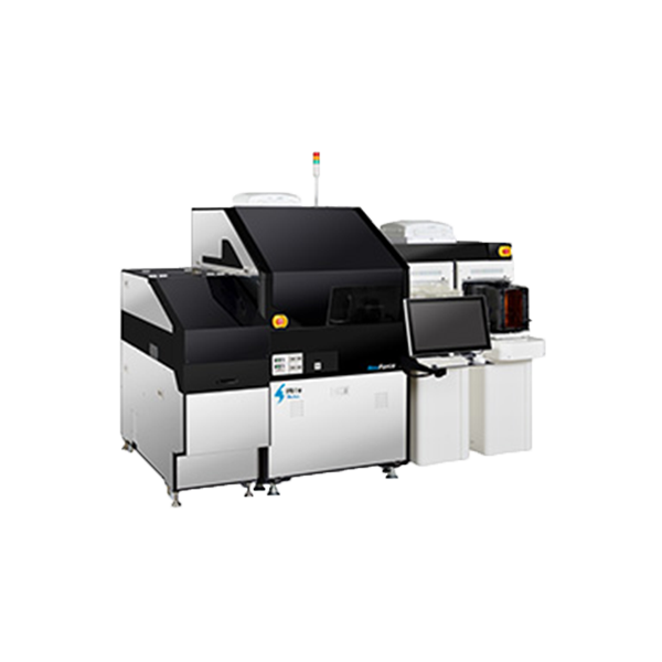

• Chip to Substrate package bonder for TCB process
• Capable of handling face down process (face up process as option)
• Capable of handling several kinds of processes such as TCB (NCP/NCF/TC-CUF), C2 and C4, and FO-WLP
• High-accuracy bonding achieved by adopting the unique Non-vibration System (NVS) technology
• Capable of handling high force up to 350N with Force Free Gantry (FFG)
• High throughput achieved by short heating and cooling time with high-speed pulse heater
• Flexibility to handle various plunge-up systems, enabling thin die handling
• Automatic product-type changeover function with capability to bond up to 4 different product-type chips, enabling 2.5D and 3D stack packaging
• Bond Process Handling Capability: TCB processes (NCP/NCF/TC-CUF), C2 and C4 processes, FO-WLP process
• Bonding Accuracy: ±2.5 μm(3σ) Based on bonding conditions at Shinkawa
• Machine UPH: UPH6,000 (C4 mode / process time not included) Based on bonding conditions at Shinkawa
• Bonding Force: 0.3–350N
※Capable of selecting bond force control method at bonding process
However, it is not capable of switching over between low force control and high force control in the identical bond profile
・Low force control mode:0.3–20N
・High force control mode:10–350N
• Bonding Tool Setting Temperature: RT–400℃ (1℃/Step, Pulse heat)
• Bonding Stage Setting Temperature: RT–200℃ (1℃/Step)
• Chip Size: □1–22 mm t=0.02–0.7 mm
• Chip Wafer Size: φ200mm, φ300mm
• Base Wafer Size: φ300 mm (φ200 mm Option)
• Bonding Direction: Face down/Face up (Option/Other conditions available on request)