


• High-accuracy bonding by unique 3D-NRS technology
• High-productivity and space-saving footprint by adopting twin-head
• High-speed thin die pick-up system with a speed of 400ms / t:20um(option) *Depending on material conditions
• Friction-free bonding head with simultaneous positional and force control for thin die stacked devices
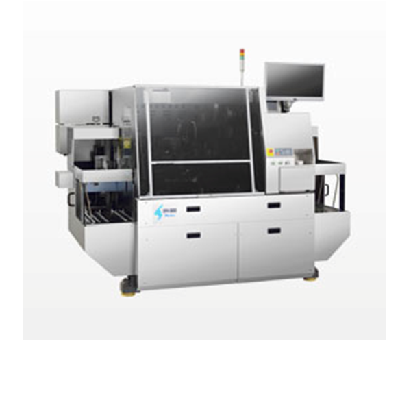
• Cleanness control with HEPA-filter and stainless steel full cover
• Equipped with die back-side camera on each bonding head, enhancing inspection function with a total of 8 cameras
• Capable of handling large substrates up to 120mm width x 300mm length
• Bonding Method: DAF bonding
• Accuracy: XY:±5μm (3σ)、θ:±0.05°(3σ) (Machine accuracy excluding material-induced factors)
• Productivity: The productivity increased by 2.5 times compared with conventional model.
(Theoretical value with Shinkawa's standard sample)
• Chip Size: □0.8 – 25mm
• Wafer Size: Maximum 12-inch
• Substrate/Leadframe Size: Width: 40 – 120mm,
• Length: 180 – 300mm,Thickness: 0.05 – 0.8mm