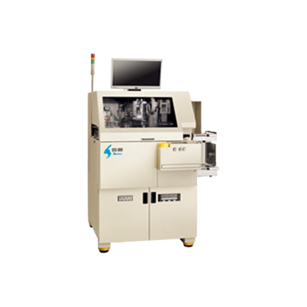
Discrete Application Die Bonder

Manufacturer:  Shinkawa

Model No.:  STC-800

Specifications

• Chip-to-Wafer package bonder for TCB process

• Capable of handling face down process (face up process as an option)

• Capable of handling several kinds of processes such as TCB (NCP/NCF/TC-CUF), C2 and C4, and FO-WLP

• High-accuracy bonding achieved by adopting the unique Non-vibration System (NVS) technology

• Capable of handling high force up to 350N with Force Free Gantry (FFG)

• High throughput achieved by short heating and cooling time with high-speed pulse heater

• Flexibility to handle various plunge-up systems, enabling thin die handling

• Automatic product-type changeover function with capability to bond up to 4 different product-type chips, enabling 2.5D and 3D stack packaging

• High-productivity and space-saving footprint by adopting multiple heads

• Bond Process Handling Capability: TCB processes (NCP/NCF/TC-CUF), C2 and C4 processes, FO-WLP process

• Bonding Accuracy: ±2.5 μm(3σ) Based on bonding conditions at Shinkawa

• Machine UPH: UPH6,000 (C4 mode / process time not included) Based on bonding conditions at Shinkawa 

• Bonding Force: 0.3–350N

• Capable of selecting bond force control method at bonding process

• However, it is not capable of switching over between low force control and high force control in the identical bond profile.

・Low force control mode:0.3–20N 

・High force control mode:10–350N  

• Bonding Tool Setting Temperature: RT–400℃ (1℃/Step, Pulse heat)

• Bonding Stage Setting Temperature: RT–200℃ (1℃/Step)

• Chip Size: □1–22 mm t=0.02–0.7 mm 

• Chip Wafer Size: φ200 mm, φ300 mm

• Base Wafer Size: φ300 mm (φ200 mm Option) /Substrate

• Bonding Direction: Face down / Face up (Option/Other conditions available on request)

Discrete Application Die Bonder

Manufacturer:   Shinkawa

Model No.:   STC-800

Specifications

• Chip-to-Wafer package bonder for TCB process

• Capable of handling face down process (face up process as an option)

• Capable of handling several kinds of processes such as TCB (NCP/NCF/TC-CUF), C2 and C4, and FO-WLP

• High-accuracy bonding achieved by adopting the unique Non-vibration System (NVS) technology

• Capable of handling high force up to 350N with Force Free Gantry (FFG)

• High throughput achieved by short heating and cooling time with high-speed pulse heater

• Flexibility to handle various plunge-up systems, enabling thin die handling

• Automatic product-type changeover function with capability to bond up to 4 different product-type chips, enabling 2.5D and 3D stack packaging

• High-productivity and space-saving footprint by adopting multiple heads

• Bond Process Handling Capability: TCB processes (NCP/NCF/TC-CUF), C2 and C4 processes, FO-WLP process

• Bonding Accuracy: ±2.5 μm(3σ) Based on bonding conditions at Shinkawa

• Machine UPH: UPH6,000 (C4 mode / process time not included) Based on bonding conditions at Shinkawa 

• Bonding Force: 0.3–350N

• Capable of selecting bond force control method at bonding process

• However, it is not capable of switching over between low force control and high force control in the identical bond profile.

・Low force control mode:0.3–20N 

・High force control mode:10–350N  

• Bonding Tool Setting Temperature: RT–400℃ (1℃/Step, Pulse heat)

• Bonding Stage Setting Temperature: RT–200℃ (1℃/Step)

• Chip Size: □1–22 mm t=0.02–0.7 mm 

• Chip Wafer Size: φ200 mm, φ300 mm

• Base Wafer Size: φ300 mm (φ200 mm Option) /Substrate

• Bonding Direction: Face down / Face up (Option/Other conditions available on request)

TOP